Why Young Engineers Ask “Why Don’t You Just 3D-Print the PCB?”

I am often asked about the electronics manufacturing services (EMS) process-and more specifically about the printed circuit board (PCB). Many engineers, especially those early in their careers, are surprised by the complexity of modern PCB fabrication: more than 100 major process steps and millions of dollars of capital equipment for drilling, plating, laminating, imaging, surface finishing, and routing.
A common question is: “Why don’t you just 3D-print the PCB?” It is a logical one, given that we routinely test 3D-printed rockets and other complex structures. The PCB should seem trivial by comparison. To answer it properly, we must understand how we arrived at today’s architecture and materials. Only then can we realistically explore the path toward additive (3D-printed) electronics.
Clarifying Ounces vs. Mils of Copper
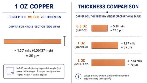
There is persistent confusion in the industry between ounces and mils of copper.
- An ounce is a unit of weight (specifically, ounces per square foot of surface area).
- A mil is a unit of thickness equal to 0.001 inch (25.4 μm).
Industry clarification: In PCB fabrication, 1 ounce of copper foil corresponds to a nominal thickness of approximately 0.00137 inches (1.37 mils) or roughly 34.8-35 μm. This is the accepted correlation used worldwide. Always distinguish between starting foil weight and finished copper thickness after plating and processing. For critical designs (impedance, current capacity, thermal performance), confirm finished thickness with your fabricator.
Brief History of the PCB and Assembly Process
Early Concepts: Before Commercial Plated Vias
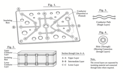
For nearly half a century after early electrical experiments, commercial products did not use plated vias or the multilayer structures we recognize today. Patents for adhering metal to non-conductive substrates date to the 1920s and earlier.
One of the earliest relevant patents was filed around 1903 by Albert Hanson (a Berliner living in London). His concept described flat conductors sandwiched between insulating layers, with holes that could be punched to allow connections to buried conductors. It essentially sketched a multi-layer idea with interlayer access-remarkably forward-looking, yet largely unknown and unused before it expired.
Austrian engineer Paul Eisler is widely regarded as the father of the modern PCB. Working in England as a refugee, he developed methods of etching copper foil to create conductive patterns. He built a radio using this technology (experiments in the late 1930s, working device around 1942) and filed key patents in 1943 (later issued as related patents covering foil techniques, powder printing, and three-dimensional circuits). Eisler’s work enabled mass-producible, reliable interconnects far superior to hand-wired “bird’s nests.”
During World War II, the U.S. Army used early printed circuit techniques (including ceramic-based approaches) in proximity fuzes. Globe Union and related work contributed to these classified military applications. After the war, the technology spread rapidly into commercial electronics.
When Plated Vias Appeared
Many early attempts created traces and holes, with components soldered into openings. True plated through-holes (PTHs) that interconnect multiple layers came later.
In the early 1960s, Hazeltine Corporation patented multiplanar (multilayer) printed circuits with conductive material deposited on the walls of perforations-essentially describing plated vias and the structures used today. Remarkably, the patent was largely theoretical at the time; contemporary manufacturing technology could not reliably produce most of the described configurations. No specific substrate was detailed, and glass/epoxy laminates arrived later. It is the combination of glass/epoxy dielectric and plated copper barrels that enabled the complex via structures of modern PCBs.
Today, patents require demonstrated reduction to practice rather than pure conceptual invention. Corporate filings were common in that era.
Creating Small Vias: Mechanical Drill vs. Laser
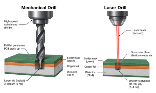
For blind, buried, HDI (high-density interconnect), and stacked vias:
- Mechanical drilling is preferred whenever possible. Modern single-spindle machines can reach approximately 200,000 RPM (compared with roughly 3,800 RPM for a typical home drill press).
- When hole size drops below about 6 mils (0.006 inch or 0.15 mm), laser drilling is required. A 6-mil drill bit is so fragile that even light air pressure can break it.
Early PCBs were single-sided. Circuitry often began as individual wires captured in phenolic resin (a hard brown material formed from phenol and formaldehyde). Innovators later saturated paper layers with resin and cured them in presses. Copper sheets were eventually laminated and etched to form traces. Many claim credit for various steps; the process evolved through parallel experimentation.
By the end of the 1960s, the basic structure of rigid PCBs had stabilized: fiberglass (glass/epoxy) supporting copper traces and copper-lined via holes, with solderable surface finishes in soldering areas and protective solder mask over the traces. This architecture has endured for more than 50 years.
Present Structure of Rigid PCBs: Why Copper and Fiberglass?
Of the core elements, the copper interconnects (traces, pads, and vias) and the fiberglass supporting structure have proven most resistant to simple substitution by 3D printing.
Copper sits at the top among common electronics metals (gold, silver, tin, nickel) for both electrical and thermal conductivity. It is abundant, relatively inexpensive, readily plated (electroless or electrolytic), and forms a strong intermetallic with tin-based solders.
Fiberglass (glass/epoxy) was chosen primarily for cost and mechanical strength rather than being purpose-engineered for PCBs. It proved serendipitously ideal:
- Very low thermal conductance.
- Strong self-bonding for multilayer lamination.
- Excellent adhesion to the plated copper barrel inside drilled holes.
Why the Present PCB and Assembly Process Has Endured: The Soldering Symbiosis
Soldering requires:
- Two surfaces that form an intermetallic with tin,
- Flux to activate surfaces and displace oxygen,
- A tin-based solder alloy, and
- Heat sufficient to exceed the alloy’s melting point.
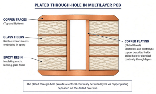
The high thermal conductivity of copper (~400 W/m·K) rapidly transfers heat through the plated barrel to the opposite side (essential for a proper through-hole fillet). Simultaneously, the low thermal conductivity of epoxy-glass acts as a thermal insulator, limiting heat loss into the laminate and preventing widespread melting of the support medium.
The major mechanical strength of a plated via comes from the copper attachment to the glass mat inside the hole. Epoxy may locally soften or melt adjacent to the barrel during soldering, but the glass fibers remain intact and hold the structure. Multilayer boards gain additional strength from the attachment of inner-layer pads.
This relationship was tested during the RoHS transition. Changing from Sn/Pb (melting point ~183-187 °C) to lead-free alloys (typically 217-228 °C) without altering the PCB laminate led to early failures from epoxy resin mass loss, reduced joint strength, brittle fracture modes, head-in-pillow defects, and increased tin whisker concerns. The system had evolved successfully over decades with limited study of the critical interaction between board and assembly process. “If it ain’t broke, don’t fix it” proved costly when one element was altered in isolation.
Where Do We Go from Here? 3D-Printed and Additive Electronics
The history lesson is clear: we must understand the interdependencies of a complex system before changing only one part.
Today, 3D-printed or additive PCBs using conductive inks exist and are commercially available for certain applications (flexible circuits, membrane switches, high-frequency boards, prototypes). Multi-material printers can deposit both conductive and dielectric materials. Progress has accelerated since 2023:
- Companies such as Nano Dimension (Dragonfly series) have demonstrated multi-layer printed boards, including 10-layer examples with embedded passives and complex vias.
- Improved conductive filaments, silver and copper nanoparticle inks, liquid metals (e.g., EGaIn), and hybrid processes have raised conductivity and reliability.
- Research into fully recyclable approaches (e.g., water-soluble substrates with recoverable conductors) and ceramic-based printed circuits for high-power applications continues.
- Environmental and economic analyses show potential advantages for certain additive processes, particularly in reduced waste and shorter supply chains, though high-performance silver inks remain costly.
However, current conductive “inks” (typically metal-filled polymers) still lag pure copper in bulk conductivity and are generally incompatible with conventional high-temperature soldering. Substrates remain largely glass/epoxy or polyimide for rigid and flex applications. Fully integrated mixed-resin structures with embedded strength materials (glass mat, carbon fiber, graphene) are not yet economically competitive for high-volume, high-reliability production.
Key questions for assembly if additive PCBs become mainstream:
- How will components be attached if traditional soldering melts the resin or fails to wet the ink?
- Will we eliminate stencil printing, SPI, and reflow, replacing them with conductive adhesives or other joining methods dispensed by the placement machine?
- How flat and dimensionally stable will the printed surface be? Will components require placement at varying depths or orientations?
- Could the entire process shrink to essentially two machines (print + place-and-bond), potentially moving prototype or even some production work back to OEMs?
- What capital, process control, and workforce skills will the EMS industry need to remain relevant?
Emerging Trends Driving Radical Change in Electronic Assembly (Updated 2026)
The focus here is on trends that will fundamentally alter equipment, processes, and the role of EMS companies.
Advances in Printable Materials for Structure and Conductance
Nanotechnology and material science continue to advance. Metal-filled inks work for low-current and low-frequency uses but are insufficient to fully replace copper for power or high-reliability applications. New conductors (improved nanoparticle systems, liquid metals, hybrid formulations) are closing the gap. Supporting substrates for non-soldered attachment are less challenging; carbon-fiber and graphene composites offer strength and light weight. One promising vision is that the “PCB” (or its successor) becomes the structural enclosure itself-integrating displays, lighting, sensors, and interconnects so that surfaces emit light or sense the environment without discrete bulbs or separate boards.
Movement Away from Silicon-Based Components
While gallium and other compounds have long been used, the next generation of organic and hybrid semiconductors offers flexibility, potential biocompatibility, and reduced environmental impact. Organic photovoltaics have reached impressive flexible efficiencies (>17% in some formats), stretchable OLEDs are advancing, and organic semiconductor-based sensors and transistors are being integrated into wearables and bioelectronics. Combined with AI, these systems can monitor and correct biological or mechanical functions in real time. Fully organic or hybrid systems that do not require high-temperature soldering could enable conformal, body-compatible electronics that current rigid silicon assemblies cannot achieve.
Miniature and Embedded “Everything”
Additive manufacturing and organic electronics enable a new form of miniaturization beyond traditional Moore’s Law scaling of silicon. Circuits can be sized and shaped to the application, embedding sensors and controls into virtually any object or biological system. This will make today’s IoT appear primitive. EMS companies must invest in new capital equipment, materials expertise, and workforce training to produce these hybrid, multi-material, highly integrated systems.
One Last Thought: The Technology Pyramid and Resilience
I have long been concerned about the modern technology pyramid, which stands on its point rather than its base. The electronic revolution is relatively recent; we continue to innovate at the top while risking loss of the foundational knowledge and tools needed to recreate the stack from scratch.
Silicon-based electronics have a fundamental vulnerability: sensitivity to electromagnetic pulses (EMP), whether terrestrial or solar. A significant event could disable vast numbers of devices. In such a scenario, engineers who understand pre-digital systems (or even older ignition systems) and who can still use basic tools and reference physical books would be essential. Can we rebuild the tools that make the tools that make the machines? Are we one major solar event away from needing to restart significant portions of the technological base?
As we add layers to the technology pyramid through additive manufacturing, organic electronics, and extreme miniaturization, preserving foundational knowledge and designing for resilience remains critical.
Conclusion
The traditional PCB-copper traces and vias in a glass-epoxy laminate, assembled with tin-based solders-has endured because of a remarkable, largely unplanned symbiosis of materials, thermal properties, and process physics. Understanding that history is essential before we successfully transition major portions of the industry to additive processes.
Progress in 3D-printed and additive electronics since 2023 is real and accelerating, particularly for prototypes, flexible/hybrid systems, and specialized applications. Full displacement of high-reliability copper/glass structures for demanding aerospace, defense, automotive, and industrial uses will require continued advances in conductivity, thermal performance, adhesion, and process economics.
At DIVaero, we continue to apply deep process knowledge to aerospace and defense electronics while monitoring these transformative trends. The industry that masters both the enduring fundamentals and the emerging additive and organic technologies will define the next era of electronics manufacturing.
Note: This article is based on a 2023 SMTA presentation by Stanley L. Bentley, P.E., with historical verification against industry sources (including IPC-related literature, patent records, and manufacturer histories) and updates reflecting 2024-2026 developments in additive manufacturing and organic electronics. Images include original presentation materials and publicly available illustrative photographs.
About the Author: Stanley L. Bentley, P.E., is Owner and Sr. Technical Director of DIVaero (DIVSYS Aerospace & Engineering LLC), an Indianapolis-area company focused on aerospace and defense electronics manufacturing, PCB assembly, testing, and legacy system sustainment. He has more than 40 years of hands-on experience across the full PCB lifecycle. The author is presently involved with the development of very high thermal conductance PCBs (on the order of 15WMK) for use with circuits requiring high pulse power that are difficult to cool with conventional techniques. He is presently producing demonstration prototypes in his PCB lab.